Analog Capacitance Meter
Collaborated with 1 other engineer to design, simulate, construct, and validate an analog capacitance meter.
Overview
In my Electronics: Introduction to Linear and Digital Circuits course, we were given 18 days to design, simulate, construct, and validate an analog capacitance meter together with a partner. The device needed to achieve at least 95% accuracy when measuring capacitance values spanning three decades (5nF to 5 µF) with a linear voltage output range of 0.5 V to 5 V. We were required to incorporate control logic for automatic switching between voltage ranges to correctly identify the capacitance range.
The planning and design phase of our project work consisted of developing a high-level block diagram, defining the design specifications, establishing preliminary component values, conceptualizing control logic with a state diagram, and setting voltage thresholds. During the analysis stage, we utilized on LTSpice to simulate individual circuit blocks and the system of circuits as a whole. Relying on the simulation results as well as our knowledge of circuit functionalities, we documented our predictions of oscillation frequency, output voltage range, current drive, and input/output impedance for each circuit block. The last phase of our project was constructing the capacitance meter circuit on a breadboard, testing the meter using capacitors of known values to debug the system, and making modifications as needed to achieve the desired accuracy.
Our device met the design goals pretty well. We produced a voltage that was within the 0.5V to 5V range for all of the capacitors we tested. We incorporated two LED sensors to indicate which capacitor decade we were in, with unique combinations of the LED lights being turned on each corresponding to 1 of the 3 decades we were testing for. The peak voltage measurements taken at the output of our circuit weren’t always 95% accurate. For the 1µF capacitor, we were about 80% accurate; for the 100nF capacitor, we were 95% accurate; for the 10nF capacitor, we were only at 75% accuracy. We still had the 2nd most accurate capacitance meter out of the 17 pairs in our class. A major contributor to this overall decreased inaccuracy was likely the analog components we were handed in the lab.
Design Considerations
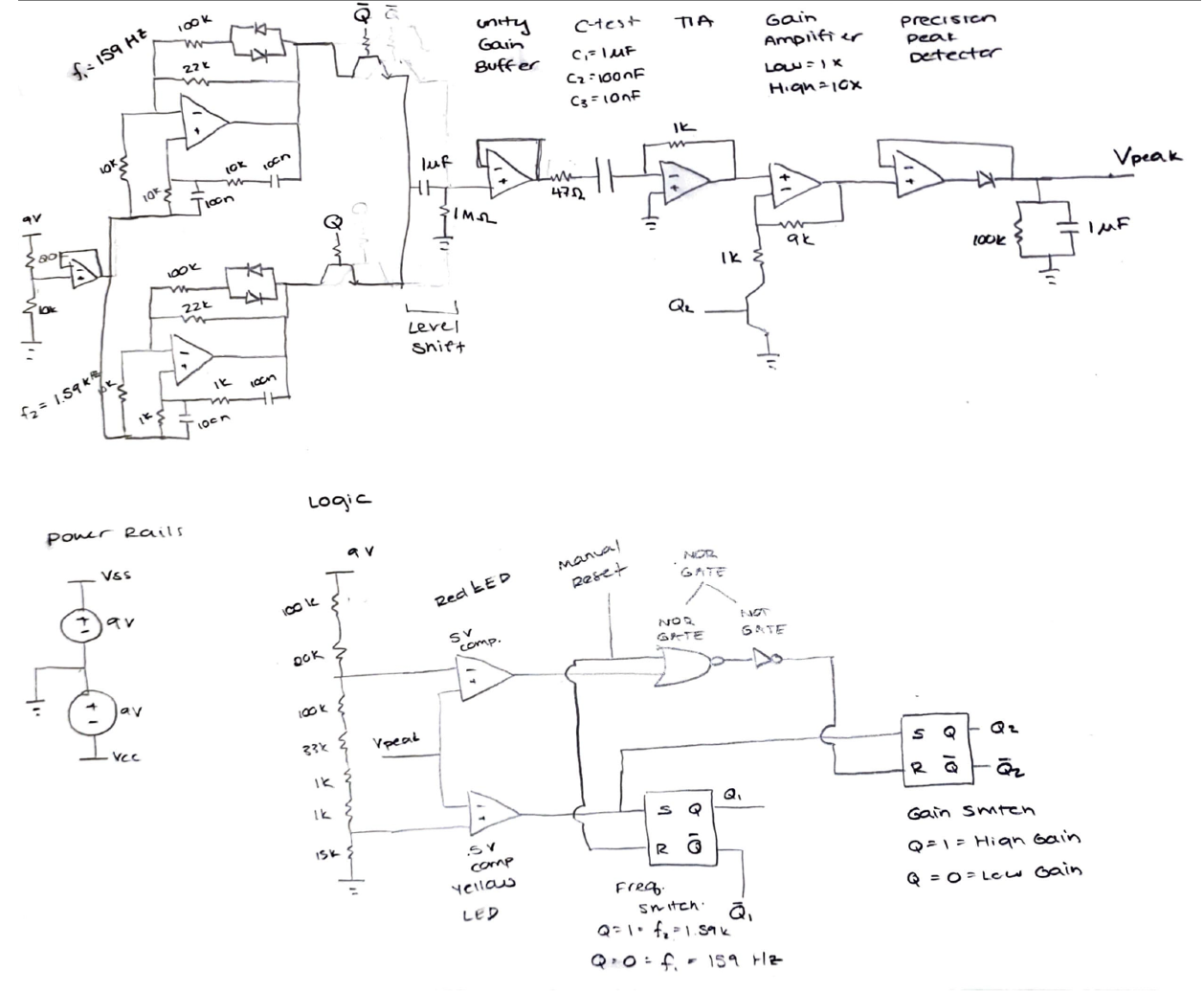
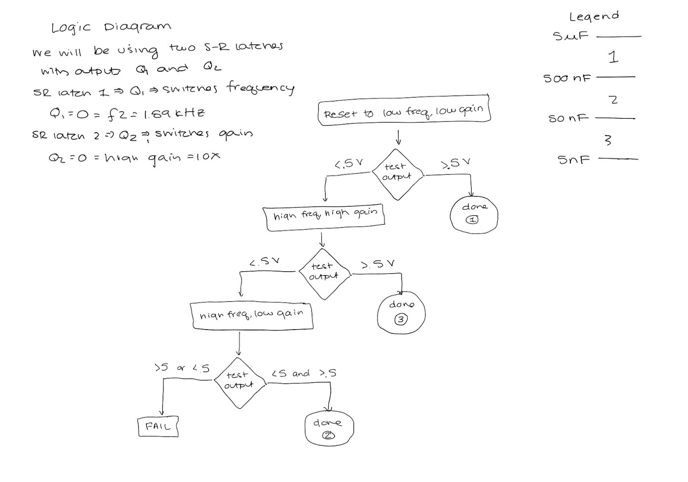
Essentially, we start in a low-frequency low gain state because we start by pressing the master reset button and the master reset button resets both of the SR Latches. If the signal from Vpeak is lower than 0.5V, the 0.5V comparator outputs a high digital signal. This digital signal sets both of our two SR Latches. The first SR Latch, the frequency SR Latch, picks a high frequency when set, as the Q output is connected to the low-frequency oscillator circuit and Qbar is connected to the high-frequency oscillator via a switch. The second SR Latch, the gain SR Latch, makes the gain circuit a 10x gain circuit when set, as Qbar is attached to the node between the second resistor and ground. This puts us in a high-frequency, high-gain state. The NOR Gate connected to the Reset port of the second SR Latch outputs a low signal either when the 5V comparator outputs high (meaning Vpeak is higher than 5V) or when the master reset button is pressed. This low signal turns into a high signal after going through the digital inverter. Finally, this high signal can reset the second SR Latch, making the gain circuit, once again, a unity gain buffer. This is the last state we test in—the high-frequency, low-gain state.
The final circuit included analog ground reference, two Wien Bridge Oscillators, a level shift, a unity gain buffer, a Trans-Impedance Amplifier, a gain amplifier, and a precision peak detector. Below is a description of each of the circuit blocks and why they were included:
Analog Ground Reference: The analog ground reference was implemented to create a 3V DC offset to both of the Wien Bridge Oscillators. This was built using a voltage divider to create the 3V DC from the 9V positive power rail, as well as an op-amp.
Wien Bridge Oscillators: To generate our input waveforms we studied multiple oscillators and ultimately landed on the Wien Bridge oscillators. We used two Wien Bridge Oscillators to create a high-frequency and a low-frequency input signal. The high-frequency signal was designed to have a frequency of 1.59kHz while the frequency of the low-frequency signal was 159Hz.
Level Shift: The purpose of the level shift was to shift the output back down to 0V from the 3V DC offset.
Unity Gain Buffer: We incorporated a unity gain buffer after the frequency generation stage to isolate this stage of the circuit, prevent loading effects, and ensure that signal integrity is maintained. The unity gain buffer uses an op-amp configured with its output connected to the inverting input, providing a voltage gain of 1 while offering high input impedance and low output impedance.
Trans-Impedance Amplifier: We know that the current going through a capacitor is equal to the product of its capacitance value and the derivative of the voltage with respect to time. A Trans-Impedance Amplifier after the device under test will convert the current signal coming out of the capacitor into a proportional voltage signal using an op-amp with a feedback resistor.
Gain Amplifier: To account for all three decades that we are testing for, while maintaining a linear voltage output range between 0.5 V and 5V, we incorporated a gain amplifier, the configuration of which allowed us to switch between unity gain and 10x gain.
Precision Peak Detector: We used the precision peak detector to extract and hold the peak voltage value of the sinusoidal waveform being output by the rest of the circuit preceding it. This peak voltage signal can then be more precisely fed into the digital logic, as well as measuring the maximum voltage corresponding to a capacitive sensor’s output.
Takeaways
Every step of this project was incredibly challenging and rewarding at the same time, marked by my first experience in building a system of circuits without structured guidance. One of the key takeaways from the project was the importance of debugging, which proved to be as critical as the design phase. This was especially evident when working with analog components that may not behave as expected. We learned that allocating sufficient time for debugging was essential for the project's success, despite the process being more intricate and time-consuming than anticipated. Ensuring the correct power supply connections was also vital; we encountered several issues due to simple errors such as connecting the power supply to incorrect nodes. Additionally, maintaining a clean and organized circuit layout, along with consistent color-coded wiring, greatly facilitated debugging and reduced confusion. Documenting the colors used for each connection allowed us to trace them back to the schematic effectively. We also discovered the necessity of avoiding fully stripped wires to prevent shorts caused by exposed sections touching each other, which became a source of unnecessary troubleshooting. If given the opportunity to repeat this project, we would adopt a more structured approach, testing each circuit block individually before integrating the digital and analog portions. This method would improve efficiency in both circuit building and debugging, as some of the additional time invested in the project was redundant and could have been avoided with continuous debugging. Furthermore, we would prioritize simplicity in our circuit design; our initial logic design included multiple NOR gates and inverters, which we later simplified while still achieving the desired functionality.


